
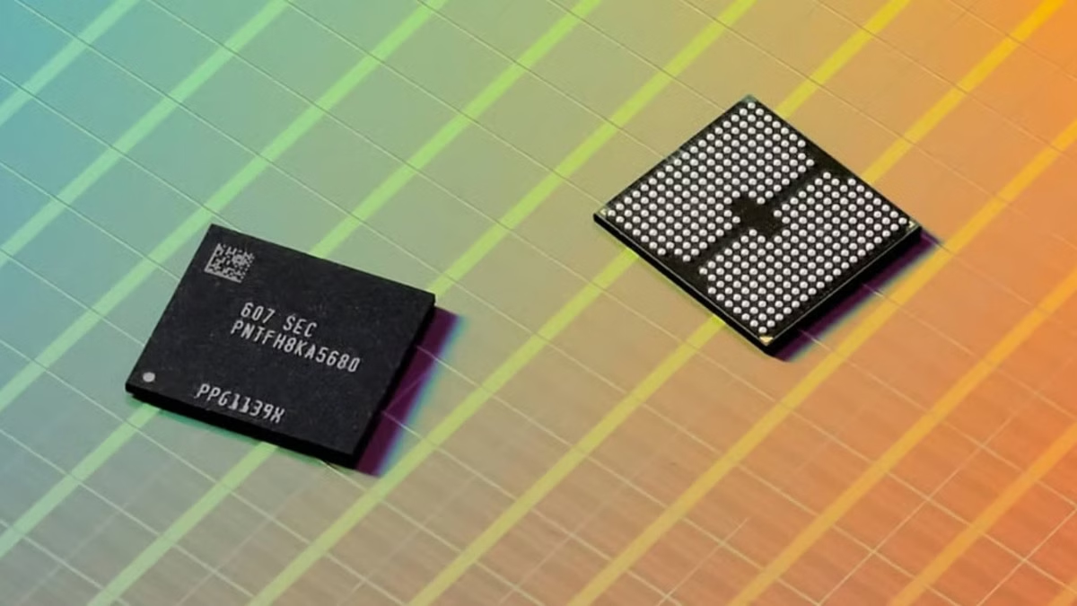
Samsung Electronics has unveiled a major advancement in artificial intelligence memory technology as the company aims to strengthen its position in the rapidly expanding AI semiconductor market. The world’s largest memory chip manufacturer introduced its latest V10 Bonding V-NAND (BV-NAND) prototype, featuring more than 400 layers and a new architecture designed to deliver higher storage density and improved performance.
The breakthrough technology was presented at the Future of Memory and Storage conference in Santa Clara, California, where Samsung showcased its vision for the next generation of high-performance memory solutions. The company said the new architecture represents a significant step toward meeting the growing computing demands created by artificial intelligence applications.
Samsung’s V10 Bonding V-NAND prototype uses an advanced wafer-bonding structure that allows multiple memory layers to be integrated more efficiently. This design enables the creation of chips with greater storage capacity while improving overall efficiency for AI workloads.
The new technology achieves approximately 58% higher density compared with previous generations, making it better suited for applications that require massive amounts of data processing. AI systems, cloud computing platforms, and advanced data centers increasingly depend on high-density memory solutions to handle complex workloads.
Artificial intelligence has created unprecedented demand for advanced semiconductor technologies. As companies develop larger AI models and deploy more powerful computing systems, memory performance has become a critical factor in improving speed, efficiency, and scalability.
Samsung’s latest innovation is designed to address these challenges by offering higher capacity and improved performance within a smaller physical footprint. The development could help data centers process larger volumes of information while reducing space and energy requirements.
The introduction of BV-NAND highlights Samsung’s continued investment in the future of memory technology. The company has been competing aggressively in the AI chip market, where demand for advanced memory products has grown significantly due to the expansion of generative AI services and enterprise artificial intelligence solutions.
High-performance memory plays an essential role in AI infrastructure because modern AI models require rapid access to large datasets. Technologies like Samsung’s advanced V-NAND solutions can help improve the efficiency of AI training, inference, and data processing operations.
The 400-plus-layer design also demonstrates the semiconductor industry’s ongoing shift toward increasingly complex chip architectures. Manufacturers are exploring new methods of stacking and connecting layers to overcome traditional limitations in memory scaling.
Samsung’s focus on wafer-bonding technology reflects a broader industry trend toward innovative manufacturing approaches. As traditional methods face physical and technical challenges, advanced packaging and stacking techniques are becoming increasingly important for future chip development.
The company’s latest prototype could play a significant role in future AI-focused products, including enterprise servers, cloud computing systems, and high-performance computing platforms. While the technology is still in the prototype stage, it provides a glimpse into the direction of next-generation memory solutions.
The growing importance of AI has intensified competition among global semiconductor companies, with manufacturers investing billions of dollars in research and development. Samsung’s continued advancements in memory technology are aimed at maintaining its leadership position while supporting the evolving needs of the AI ecosystem.
As artificial intelligence adoption accelerates worldwide, demand for faster, denser, and more efficient memory solutions is expected to continue rising. Samsung’s 400-layer BV-NAND technology represents a significant milestone in the company’s efforts to build the infrastructure needed for the next era of intelligent computing.